3D Plus has received the 2007 EUREKA Lynx Award for outstanding technological and commercial achievement. This trophy is awarded by the highly successful EUREKA WALPACK project, which developes high-density, 3D chip-stacking technology for cost-effective system-in-package devices. The award was presented at EUREKA’s high-level Group gala dinner, in Rome.
“Winning the EUREKA Lynx award is very important to us,” says 3D Plus’ CEO Christian Val. “It provides recognition of our success and will help in all our marketing, as well as in communications with the public authorities in France.”
The company established the project (under its PIDEA Cluster) with French and Polish processing and test equipment manufacturers, potential customers and research institutes. “EUREKA labelling enabled us to put together the consortium faster and with less effort than under the EU Framework Programme,” explains Mr Val.
Overall, the technological advances and industrial contacts made in the EUREKA project enabled 3D Plus to develop and market industrially relevant products quickly. This also helped raise the company’s visibility to access the funding it needed.
3D interconnection technology for microelectronics was developed by the Thales defence electronics group in 1989 for aerospace applications. Two Thales engineers then set up 3D Plus in 1996 to exploit the technology more widely; it is the only company in Europe to specialise in this technology.
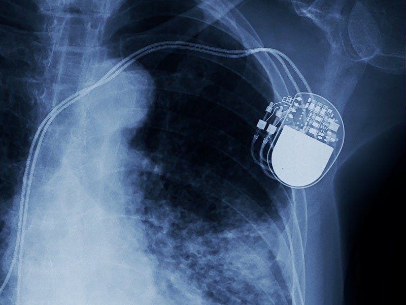
Sustained R&D has made it possible to offer smaller devices with increased efficiency for use in automotive electronics, mobile phones and high-capacity smart cards to biomedical devices that can be embedded in the human body.
Growing pressure to reduce the size of microelectronics while improving performance and reliability has led to extensive use of System-In-Package (SIP) devices. These combine a range of optimised Integrated Circuit (IC) and passive devices in a single module.
Major chipmakers have attempted to make SIPs by stacking complete wafers on top of each other, interconnected through holes in the silicon substrate. However, this is limited to wafers from the same manufacturer with all IC dies having the same dimensions. It also requires modifications to the wafer and yield is poor as individual chips cannot be guaranteed.
The resulting Walpack process assembles wafers from a mixture of fully tested chips of any size and stacks the rebuilt wafers on top of each other, inside a polymer package. A standard pick-and-place machine assembles the dies, with laser etching employed for interconnections. Advantages include use of standard chip dies with high yields as all chips are tested before assembly.
Following the EUREKA project, 3D Plus signed an agreement with NXP – formerly Philips Semiconductors – to develop the process further. NXP now manufactures modules for 3D Plus as well as its own applications. Even before the end of the project, 3D Plus attracted interest from the biomedical devices industry. Also, 3D Plus is developing high capacity smart cards for a market with major potential – consumption of 400 million cards a year is forecast by 2010.


